Skip to content

Gary Hilson

Freelance B2B / Technology Writer / Storyteller
Menu
  • Home
  • About
    • Dancing
    • Photography
    • Resume
  • Bylines
  • Clients
  • Contact
  • Services

Tag: technology

CXL Update Emphasizes Security [Byline]

January 3, 2025 / Gary Hilson

The latest point release to the Compute Express Link specification aims to optimize monitoring and management and enhance functionality for operating systems and applications—all while extending security.

The updates reflect the rapid growth of AI in the data center, even though the coherent connectivity protocol was conceived before the AI boom took off.

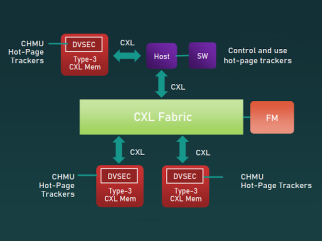
The latest CXL update, CXL 3.2, adds several monitoring and management capabilities, including a CXL hot-page monitoring unit (CHMU) for memory tiering, common event record, compatibility with PCIe management message pass through (MMPT) and CXL online firmware (FW) activation.

CHMU enables software to identify hot pages in second-tier memory and migrate them to first tier, such as DDR DRAM, to improve power and performance of the tiered memory solution. New common event record capabilities allow for improved granularity, monitoring precision and management of complex CXL device configurations, which enhances overall system performance and resource allocation.

Additional functionality in 3.2 includes post package repair (PPR) enhancements and performance monitoring events for CXL memory devices.

The trusted security protocol (TSP) features first introduced in CXL 3.1 are in line with confidential computing concepts pioneered by Intel that predate CXL and allow for virtualization-based trusted execution environments to host confidential computing workloads. Additional TSP features in 3.2 include IDE protection for late poison messages, which improves security for CXL-attached systems by allowing late poison messaging authentication using IDE.

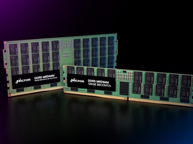
The CXL interconnect has evolved rapidly since its debut in 2019 with three sub-protocols: CXL.io, CXL.cache and CXL.memory. CXL.io is necessary for I/O instructions. The first iteration supported direct attachment of memory, while 2.0 added the capability to attach memory to a pool of processors, allowing for the use of storage-class memory or persistent memory, or tiers of memory with different performances and cost structures.

CXL 3.0 supports more disaggregation with advanced switching and fabric capabilities, efficient peer-to-peer communications, and fine-grained resource sharing across multiple compute domains.

Read the full EE Times story

Gary Hilson is a freelance writer with a focus on B2B technology, including information technology, cybersecurity, and semiconductors.

Micron, Intel Bring MRDIMM Modules to Market

August 16, 2024 / Gary Hilson

Micron Technology’s latest memory offering is a collaboration with Intel to address memory-intensive data center applications like AI and high-performance computing (HPC).

Micron presented its multiplexed rank dual inline memory modules (MRDIMMs). This first generation of MRDIMMs will enable customers to run increasingly demanding workloads with support for a wide capacity range from 32 GB to 256 GB in standard and tall form factors (TFF), which are suitable for high-performance 1U and 2U servers, and are compatible with Intel Xeon 6 processors.

For applications requiring more than 128 GB of memory per DIMM slot, Vaidyanathan said Micron MRDIMMs outperform current TSV RDIMMs, while the TFF modules feature an improved thermal design that reduces DRAM temperatures by up to 20 degrees Celsius at the same power and airflow to enable more efficient cooling in the data center.

Over the last decade, compute performance has been delivered through rapid growth in core count to grow system bandwidth, but the challenge has been maintaining bandwidth per core and getting it to curve upward. The MRDIMM is Micron’s effort to reduce the decline in bandwidth per core, he added.

Compared with RDIMMs, MRDIMMs increase in effective memory bandwidth as much as 39% and latency by 40%, while offering 15% better bus efficiency.

Micron and Intel confirmed that its MRDIMM product would be in alignment with industry standards—it implements DDR5 physical and electrical standards that scales both bandwidth and capacity per core to future-proof compute systems.

The Intel/Micron launch came out ahead of the JEDEC Solid State Technology Association revealing key details about its upcoming standards for DDR5 MRDIMMs, which it said would enable applications to exceed DDR5 RDIMM data rates. Other planned features in the JEDEC MRDIMM standard will include platform compatibility with RDIMM for flexible end-user bandwidth configuration, use of standard DDR5 DIMM components like DRAM, DIMM form factor and pinout, serial presence detect (SPD), power management integrated circuits (PMIC), and temperatures sensors (TS) for ease of adoption.

JEDEC said there are also plans to support the tall MRDIMM form factor to offer higher bandwidth and capacity without changes to the DRAM package. By going taller, it is possible to enable twice the number of DRAM single-die packages to be mounted on the DIMM without the need for 3DS packaging.

Read my full story on EE Times.

Gary Hilson is a freelance writer with a focus on B2B technology, including information technology, cybersecurity, and semiconductors.

DPUs take the pressure off purpose-focused processes [Byline]

August 14, 2024 / Gary Hilson

Data processing units (DPUs) are having a moment.

As artificial intelligence (AI), high performance computing (HPC), increasingly complex cloud architectures and security demands put more pressure on central processing units (CPUs), and graphics processing units (GPUs), DPUs have stepped up their game.

In baseball parlance, DPUs can be seen as a “utility player,” in that they can be deployed in different ways to support workload-focused players – the CPUs and GPUs. DPUs can trace their history to the Smart network interface card (SmartNIC), which were initially designed to offload some network functions from the CPU to improve network traffic flow.

But traditional SmartNICs aren’t smart enough proceed the high volumes and different patterns of data that DPUs can. The democratization of AI through ChatGPT has put a lot of pressure on the backend as frontend users began consuming it faster – once it hit a tipping point, everyone was using it. Not all DPUs are created equal however, and AI is just one use case that’s driving their adoption.

One position DPUs can play is security. In September 2022, Nvidia introduced a DPU designed to implement zero-trust security distributed computing environments, both in the data center and at the edge. Nvidia’s BlueField-2 DPUs were specifically tailored to be used Dell PowerEdge systems with the aim of improving the performance of virtualized workloads based on VMware vSphere 8.

Nvidia’s Bluefield-3, meanwhile, is the equivalent of 300 CPU cores, and it employs purpose-built accelerators to handle storage, security, networking and steering traffic.

The next generation of AI is AI agents talking to other AI agents, and DPUs play a key role in automation and scalability while humans continue to increasingly interact with AI.  Nvidia is building out a microservices platform, NIM, that leverage DPUs to orchestrate AI interactions, providing containers to self-host GPU-accelerated inferencing microservices for pretrained and customized AI models.

The utility of DPUs in modern AI data centers has meant that other players beyond semiconductor vendors are seeing the value of owning their own DPU technology. Microsoft acquired Fungible to integrate its DPU technology into its data center infrastructure – it was already using DPUs in Azure, and there are plenty of options. Aside from Nvidia, Intel, Broadcom and AMD all have DPU offerings. Amazon Web Services, meanwhile, has its own DPUs, dubbed “Nitro.”

AMD bulked up its DPU capabilities in 2022 with the acquisition of Pensando and its distributed services platform, which had a footing in Azure, IBM Cloud and Oracle Cloud. The Pensando acquisition means AMD finds its DPU adopted in several hyperscale cloud providers. It has also been incorporated into smart switches from Aruba and Cisco.

Taking on front-end networking functions to securely connect to the GPU continues to be a key role for DPUs, as well as enabling secure isolation in multi-tenant hyperscale cloud data centers. The DPU can also accelerate storage access and speed up data ingestion – the increased volumes of training data are driving speed and performance requirements, and hence more offloading to the DPU.

With the explosive growth of generative AI, networking is the currently bottleneck as the number of GPUs in data centers grow, which is why DPUs are essentially for managing data traffic and taking on functions so the GPUs can focus on application workloads.

Read my full story on Fierce Electronics.

Gary Hilson is a freelance writer with a focus on B2B technology, including information technology, cybersecurity, and semiconductors.

CXL Efforts Focus on Memory Expansion [Byline]

June 4, 2024 / Gary Hilson

An initial promise of the Compute Express Link (CXL) protocol was to put idled, orphaned memory to good use, but as the standard evolved to its third iteration, recent product offerings have been focused on memory expansion.

SMART Modular Technologies recently unveiled its new family of CXL-enabled add-in cards (AICs), which support industry standard DDR5 DIMMs with 4-DIMM and 8-DIMM options. The AICs allow up to 4TB of memory to be added to servers in the data center. The company has spent the last year putting together these products with the aim of making them plug and play.

SMART Modular’s AICs are built using CXL controllers to eliminate memory bandwidth bottlenecks and capacity constraints and aimed at enabling compute-intensive workloads like AI, machine learning (ML) and high-performance computing (HPC) uses—all of which need larger amounts of high-speed memory that outpace what current servers can accommodate.

The introduction of SMART Modular’s AICs comes at a time where the company is seeing two basic needs emerging, with the near-term one being a “compute memory performance capacity gap.”

The other trend is memory disaggregation. The problem with memory disaggregation has been lack of standards. CXL helps with that, and then networking technology has improved significantly.

CXL overcomes the need to add more CPUs in a server environment, which is an expensive path to adding performance. The idea with SMART Modular’s AICs is that they can be in an off-the-shelf server.

Micron Technology is another early CXL mover, and its CXL CZ120 memory expansion module speaks to the trend toward adding more memory into a server to meet the demands of AI workloads rather than overprovision GPUs.

The company first introduced its CXL CZ120 memory expansion modules in August 2023, and now the module has hit a key qualification sample milestone. The CZ120 has undergone substantial hardware testing for reliability, quality, and performance across CPU providers and OEMs, as well software testing for compatibility and compliance with operating system and hypervisor vendors.

Read the full story on EE Times.

Gary Hilson is a freelance writer with a focus on B2B technology, including information technology, cybersecurity, and semiconductors.

Canadian University Augments Solar Panels to Improve Output [Byline]

May 30, 2024 / Gary Hilson

Researchers in Canada’s national capital have devised a smart approach to optimize the effectiveness of solar panels by enhancing them with artificial ground reflectors.

The University of Ottawa’s SUNLAB collaborated with the National Renewable Energy Laboratory (NREL) in Golden, Colorado, to study how reflective ground covers affect solar energy output.

The research found that placing reflective surfaces under solar panels can increase their energy output by up to 4.5%. It involved pairing high ground reflectivity with bifacial solar modules, paired with high ground reflectivity.

Solar power can be some of the cheapest power in the world, especially in sun drenched regions, such as Saudi Arabia or Quatar. But other countries like the United States and Canada have different weather patterns.

The research findings are particularly significant in Canada, where snow cover persists for three to four months of the year in major cities like Ottawa and Toronto, and 65% of the country’s vast landmass experiences snow cover for over half the year. Additionally, given that approximately 4% of the world’s land areas are classified as sandy deserts, this finding has global applications.

The efficiency of most solar panels ranges from 20% to 25%, and panel materials have evolved in the last five to 10 years from aluminum back surface field to passivated emitter and rear contact (PERC), which is much more efficient with only minor changes to the manufacturing process.

PERC cells can be made bifacial more easily, which has facilitated the production of bifacial modules globally.

The SUNLAB study at NREL site looked at the effect of high albedo (70% reflective) artificial reflectors on single-axis-tracked bifacial photovoltaic systems through ray-trace modeling and field measurements. The researchers tested a range of reflector configurations by varying reflector size and placement and demonstrated that reflectors increased daily energy yield up to 6.2% relative to natural albedo for PERC modules.

Read my full story for EE Times.

Gary Hilson is a freelance writer with a focus on B2B technology, including information technology, cybersecurity, and semiconductors.

4DS Plots ReRAM Roadmap [Byline]

May 23, 2024 / Gary Hilson

4DS Memory Limited has broken its radio silence to lay out its go-forward plans for its Resistive RAM (ReRAM) technology.

The company said its interface switching capabilities based on PCMO (Praseodymium, Calcium, Manganese, Oxygen) delivers significant advantages over other filamentary ReRAM technologies, making its high-bandwidth, high-endurance persistent memory suitable for AI, big data and neural net applications.

4DS’ ReRAM requires no refresh within its persistence window and can be “refreshed” within the DRAM operating window, which makes it able provide high bandwidth and high endurance while using less energy.

He said the company’s roadmap includes a development agreement with Belgium-based imec for a 20-nm Mb chip with 1.6B elements to be run at imec in 2024.

4DS’ use of PCMO makes its ReRAM different from other ReRAM makers, in that the switching mechanism is based on the interface characteristics of the cell—the entire interface area is involved in the switching. Other ReRAM makers use a filamentary wire, which proves long cell retention.

In PCMO ReRAM, oxygen ions are moved in and out of the cell by the electric field pulse. When this oxygen is present, the cell conducts, and it is said to be SET. When the oxygen is removed, the current path is lost, and it is said to be RESET.

A key advantage of 4DS’ PCMO-based interface is that the pulse response is very fast, and endurance is higher.

4DS is focused on two goals this year: It’s continuing to work with imec to fab out a 20-nm cell to make it competitive with other ReRAM technologies, and the company sees no point in waiting to strike potential partnerships and start new application discussions.

Using praseodymium is a unique choice by 4DS, and the company could encounter issues getting a praseodymium-based process to a maturity level that will allow it to be put into mass production and drive out the costs.

There are a few ReRAM devices available at present for special applications, with Fujitsu Semiconductor and Renesas offering standalone products.

Weebit Nano began working to commercialize SiOx ReRAM technology developed by Rice University, with the goal of avoiding troubles other technologies had by using materials that would not create issues in a standard CMOS logic fab, such as silver or magnetic materials. The company has advanced its technology several new generations and is no longer purely SiOx. In early 2020, Weebit Nano said it was looking to ramp up its discrete ReRAM efforts based on customer demand.

Read the full story for EE Times.

Gary Hilson is a freelance writer with a focus on B2B technology, including information technology, cybersecurity, and semiconductors.

GDDR7 Adds Headroom to Meet AI Pressures [Byline]

May 13, 2024 / Gary Hilson

Recent advances in artificial intelligence may appear revolutionary, but JEDEC is keeping an evolutionary approach for Graphics Double Data Rate (GDDR) standards, even as it’s being increasingly used for AI applications.

The JEDEC Solid State Technology Association’s GDDR7 standard continues the generation-to-generation tradition of double the bandwidth and double the capacity while keeping a lid on power consumption.

The latest iteration of GDDR offers twice the bandwidth of its predecessor, reaching up to 192 GB/s per device. GDDR7 doubles the number of independent channels, from two in GDDR6 to four.

It’s also the first JEDEC standard DRAM to use the pulse-amplitude modulation (PAM) interface for high-frequency operations. Using a PAM3 interface improves the signal-to-noise ratio for high-frequency operation while enhancing energy efficiency. PAM3 also offers a higher data transmission rate per cycle, resulting in improved performance versus the traditional non-return-to-zero (NRZ) interface.

GDDR7 addresses the industry’s need for reliability, availability and serviceability (RAS) by incorporating the latest data integrity features, including on-die error-correction coding with real-time reporting, data poison, Error check and Scrub, and command address parity with command blocking (CAPARBLK).

With companies like Micron Technology selling out of HBM3, GDDR can be a viable alternative for some AI workloads, and AI demands are shaping the evolution of GDDR. One of the reasons GDDR has found uses beyond its initial target market is its ability to do matrix algebra, which helps GPUs handle AI workloads and computer-generated special effects.

GPU maker Nvidia wanted a faster, more reliable memory—hence, the adoption of PAM, as transmitting data at super-fast rates means channel integrity becomes a bigger concern.

Read my full story for EE Times.

Gary Hilson is a freelance writer with a focus on B2B technology, including information technology, cybersecurity, and semiconductors.

Texas Chip Companies Pivot to Leverage Apprenticeships [Bylines]

May 8, 2024 / Gary Hilson

Chip companies expanding their footprint in Texas must change how they approach talent intake as the semiconductor industry circles back to leveraging apprenticeships. They also educate the broader workforce on the opportunities available and how the industry underpins people’s daily lives.

In the second of two panel discussions hosted by the National Institute of Innovation and Technology (NIIT), semiconductor companies growing their footprint in Texas are transforming their culture to focus on skills over experience and allow for different types of apprenticeships.

ManpowerGroup understands the realities of the talent market, and thousands of people come into its offices daily trying to figure out their career paths. It has greatly leveraged NIIT to help people migrate from a manufacturing job to one in semiconductors through emerging apprenticeship programs.

Many companies hire full-time employees from contingent labor—it’s a massive avenue for people to get hired by corporations. A notable shift for ManpowerGroup as it supports semiconductor and advanced manufacturing companies is hiring for skills rather than just experience.

Another new challenge is that chip companies are no longer just competing with each other for talent—other sectors, such as automotive and other technology companies, want the same skillsets. Applied Materials, which collaborates with staffing companies like ManpowerGroup, must now compete with household brand names, and a registered apprentice program was part of the solution by offering more flexible pathways to improve the talent pool.

Flexibility is beneficial for other companies operating in Texas, such as NXP Semiconductors, which is upscaling its current workforce thanks to the work of schools like Austin Community College District, which takes on the group sponsorship aspect by handling monitoring and reporting on apprenticeship progress, as well as collaboration with NIIT and regional workforce development organizations.

GlobalFoundries, meanwhile has developed a unified competency model that led to a talent hub, which was a relatively new skill for the company, but it now has several hundred apprentices across its two U.S. fabs.

Read my full story for EE Times.

Gary Hilson is a freelance writer with a focus on B2B technology, including information technology, cybersecurity, and semiconductors.

Smarter MCUs Keep AI at the Edge [Byline]

May 1, 2024 / Gary Hilson

As the edge gets smarter, the challenge becomes increasing machine learning (ML) and inference without spiking power consumption—microcontrollers (MCUs) optimized for edge AI applications are important pieces of the puzzle.

Infineon Technologies’ PSOC Edge MCU series is aimed at developers looking to bring new ML-enabled internet of things, consumer and industrial applications to market. The E81, E83 and E84 options focus on usability.

The PSOC MCU series has an Arm Cortex-M55 architecture, which is augmented with Helium DSP support alongside Arm Ethos-U55 and Cortex-M33. All of this is integrated with Infineon’s proprietary hardware accelerator, NNLite, which is designed for neural network acceleration.

At the high end of the series, the E84 is aimed at graphics-enabled applications, such as fitness wearables, high-end smart thermostats or smart locks, allowing more ML to be done on-chip. Many applications are sensor-based to support anomaly detection and predictive maintenance in industrial settings, as well as to detect people when they walk into the room for security or environmental control purposes.

Like Infineon, Ambiq is looking to make the edge smarter without consuming more power. It recently launched the Apollo510, the first in its Apollo5 SoC series, to support endpoint AI, including speech, vision, health and industrial AI models, on battery-powered devices.

Apollo510’s hardware and software use the Arm Cortex-M55 CPU with Arm Helium to reach processing speeds up to 250 MHz and achieve up to 10× better latency than its predecessor, the Apollo4. Like Infineon, Ambiq is eyeing energy efficiency to support sophisticated speech, vision, health and industrial AI models on battery-powered devices.

The introduction of new MCUs to support edge AI comes at a time when generative AI (GenAI) is getting most of the attention, despite representing a small percentage of AI that’s being deployed.

Read my full story for EE Times.

Gary Hilson is a freelance writer with a focus on B2B technology, including information technology, cybersecurity, and semiconductors.

Apprenticeships Aim to Meet Texas Chip Sector Talent Demands [Byline]

April 18, 2024 / Gary Hilson

The graying of the semiconductor workforce as onshore manufacturing ramps up means the days of chip companies poaching each other’s talent are numbered—their local communities must develop talent through the collaboration of schools and workforce development organizations.

In the first of two panel discussions hosted by the National Institute of Innovation and Technology (NIIT), those collaborating to help build the talent pipeline for Texas’s semiconductor and advanced manufacturing sectors said they are working to deliver flexible options for apprenticeships to meet the demand for skilled workers with options that allow apprentices to earn a living while learning.

Austin Community College District has been collaborating with workforce development organizations and semiconductor companies to create entry pathways at various points and equip students with the right skills, especially in manufacturing.

Austin Community College District is increasingly giving tours to middle school students to expose them early to programs that will set them on a career path in semiconductors and advanced manufacturing.

The college’s Make It Center provides guests of all ages a chance to experience a wide range of experiences to pique their interest in advanced manufacturing careers, including an area dubbed “The Forge,” where they can use 3D printing, laser cutters and vacuum formers to create career-related projects. There are also virtual-reality simulations that allow users to “try out” different careers by immersing themselves in various job sites.

Read my full story on EE Times.

Gary Hilson is a freelance writer with a focus on B2B technology, including information technology, cybersecurity, and semiconductors.

Posts pagination

« Previous 1 2 3 … 16 Next »

Recent Posts

  • Remembering Star Trek Author Peter David
  • PCIe 7.0 Keeps Pace with AI Demands [Byline]
  • Quantum sensors promise precision, now, in medical & aerospace [Byline]
  • AI Demand Drives Disaggregated Storage [Byline]
  • SoCs Get a Helping Hand from AI Platform FlexGen [Byline]
  • Canada Funds Quantum Auto Security Research [Byline]
  • Micron Drives Down DRAM Power [Byline]
  • Canadian Firm Unveils Quantum Error Correction Codes [Byline]
  • PCIe Gains Automotive Mileage [Byline]
  • Onsemi’s Treo Taps Weebit ReRAM [Byline]

Recent Posts

  • Remembering Star Trek Author Peter David
  • PCIe 7.0 Keeps Pace with AI Demands [Byline]
  • Quantum sensors promise precision, now, in medical & aerospace [Byline]
Powered by WordPress | Theme by Themehaus