Skip to content

Gary Hilson

Freelance B2B / Technology Writer / Storyteller
Menu
  • Home
  • About
    • Dancing
    • Photography
    • Resume
  • Bylines
  • Clients
  • Contact
  • Services

Category: Bylines

HPC pushes quantum computing capabilities forward [Byline]

April 16, 2024 / Gary Hilson

If you’re placing bets on whether quantum computing or high-performance computing (HPC) will come up on top, the answer is both.

Comparing the two is akin to comparing apples and oranges – each has its own strengths, and these strengths dictate what problems you should throw at them. Even if the best choice is a quantum computer, it’s going to need an HPC to work effectively.

Many algorithms, such as Shor’s algorithm, would take a million years on a supercomputer no matter how advanced it was. Because of its nature, a quantum computer is better suited for cryptography, which is a key driver of government interest – it has the potential to break existing encryption. Other domains that have a keen interest in quantum computing capabilities are chemistry, materials research, and Wall Street to chart finance scenarios.

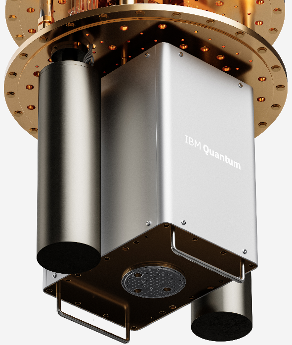
At the heart of quantum computing hardware is a qubit chip. Qubits are very fragile, and they lose their information very quickly. This loss can occur within microseconds, and that is why a classical HPC is complementary to a quantum system – a traditional supercomputer is required to do the necessary error correction.

Some problems are naturally quantum problems, such as chemistry, and not all problems are one or the other – parts of a difficult application might be farmed out to a quantum computer while others are best solved by a classical supercomputer. A quantum computer can be viewed as an accelerator of an HPC system.

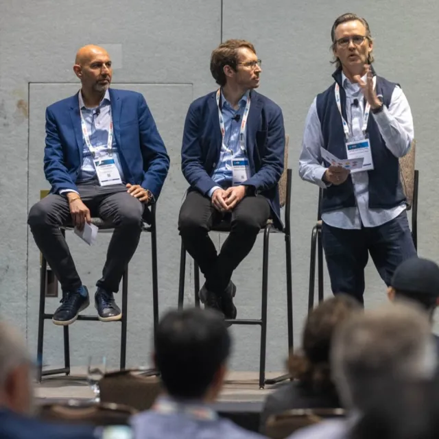
Universities play a key role in helping to develop quantum computing technologies. An interdisciplinary team at UMass Amherst is responsible for designing the infrastructure to support future city-scale quantum networks, one of four core thrust areas overseen by the National Science Foundation’s Center for Quantum Networks.

Both Intel and IBM are collaborating with universities to advance quantum computing. More than 100 institutions are members of the IBM Quantum Network, including Cern, and several have dedicated systems.

Read my full story for Fierce Electronics.

Gary Hilson is a freelance writer with a focus on B2B technology, including information technology, cybersecurity, and semiconductors.

Proprietary Memories Are a High-Risk Endeavor [Byline]

April 1, 2024 / Gary Hilson

Semiconductor technologies live and die by industry standards, but are there times when it makes sense to build a heavily customized—even proprietary—memory device?

The chip sector is replete with standards organizations that guide the evolution of widely adopted memory devices. JEDEC is responsible for DRAM, LPPDR, GDDR and high-bandwidth memory (HBM), among others. The Peripheral Component Interconnect Express Special Interest Group takes care of the most ubiquitous protocol for data movement, while NVMe Express and the CXL Consortium built their specifications with PCIe as their foundation. Most recently, the UCIe was developed to bring best practices to chiplets.

The highway of DRAM technologies is littered with the roadkill of non-JEDEC-standard memories. If something isn’t JEDEC-standard, or if a DRAM vendor tries to go it alone with something that they want to differentiate with, it’s going to die.

Among the many abandoned memories that never saw widespread use are Micron Technology’s HBM competitor, Hybrid Memory Cube, and Rambus’s virtual-channel DRAM, even though the latter had the backing of Intel.

The value of a standardized memory device is that it can be multi-sourced—an SK Hynix product will plug into the same socket as a Micron product.

That’s not to say some vendors aren’t offering special features. There will be DRAM vendors that will have their own special features that they unlock for special customers, and it’s still standard DRAM.

Some memories that are developed by more than one vendor may show potential but are subsequently abandoned by all but one of the vendors. Reduced-latency DRAM was initially developed by Infineon Technologies in the late 1990s; Micron was subsequently brought in as a development partner and a second source, but Infineon opted to exit the market.

The challenge of being the sole source of a memory product that has a strong customer base—especially if it’s a Tier 1 customer—is that it’s difficult to end-of-life the product.

Read my full story for EE Times.

Gary Hilson is a freelance writer with a focus on B2B technology, including information technology, cybersecurity, and semiconductors.

AI-Enabled Digital Twins Boost Productivity, Sustainability [Byline]

March 19, 2024 / Gary Hilson

Digital twins aren’t a new tool for the chip industry, but they are getting democratized to a point where they are more accessible for a broader set of commercial applications.

The ability to ingest more, higher-quality data from a wider array of sources and the application of artificial intelligence is helping to extend digital twins beyond product design to virtually envision manufacturing environments, which will reduce waste as well as contribute to meeting sustainability goals. And as the chip industry ramps up U.S. onshore manufacturing in the wake of the CHIPS Act, digital twins are poised to be a critical tool for workforce development while also accelerating productivity.

In early February 2024, the National Institute of Standards and Technology (NIST) announced its intent to create a new semiconductor manufacturing institute that will use digital twin technology for production, packaging and assembly. NIST is looking to corral curriculum and best practices through its CHIPS Research and Development Office to launch a competition for a new public-private Manufacturing USA Institute.

Digital twins are more effective when silos of information are eliminated, Grieves added. “Depending on what functional area they were in, you wound up with huge inefficiencies or the inability to optimize the entire process.”

Expanding the use of digital twins out to manufacturing facilities is the natural evolution of the virtual approach the chip industry has used for decades. Digital twins are being extended to visualize equipment and manufacturing facilities before they are built, then optimized once they are in production.

Digital twins can be used to build anything, so why not the manufacturing facilities that produce semiconductors—not just the devices themselves?

Building a digital twin of a fab allows for the modeling of the manufacturing of the chip, making it possible to optimize a facility before concrete is ever poured.
A digital twin does more than simulate the manufacturing process. It also optimizes all the electricity, water and chemicals being used, which helps to achieve sustainability goals.

Read my full story for EE Times.

Gary Hilson is a freelance writer with a focus on B2B technology, including information technology, cybersecurity, and semiconductors.

TSMC, NXP Scale Up Apprenticeships [Byline]

March 14, 2024 / Gary Hilson

To help meet the demands of new fabs being built in the United States, apprenticeships are emerging as a key strategy for scaling up the talent pipeline.

Taiwan Semiconductor Manufacturing Company (TSMC), for example, sees apprenticeships as critical to supporting its workforce needs as it looks to staff two big fabs.

Developing people—giving them the skills and the on-the-job experience they’ll need to secure a permanent post—takes time, especially because there are unique skills needed that aren’t immediately available. 

TSMC’s recently announced apprenticeship program in the Phoenix area focuses on developing people for a facility technician role by providing 2,000 hours of on-the-job training in four key skills areas: water treatment, gas and chemicals, electrical, and mechanical. Courses are provided by TSMC’s technical-instruction partner, Maricopa Community Colleges.

Mentorship is critical to the process: Apprentices are paired with mentors for one-on-one guidance.

TSMC identified technicians as a focus area based on its hiring needs over the next few years. The company is working with the entities in Arizona that are responsible for workforce development in the state and its various municipalities, including the Workforce Arizona Council.

NXP Semiconductor has also been working with Maricopa since early last year. The company began looking at developing apprenticeship programs in mid-2022. NIIT has helped the company map out the process for developing a semiconductor equipment technician apprenticeship, which encompasses multiple specialty areas.

Apprenticeships fall into NIIT’s broader responsibility of executing a national strategy to build the talent pipeline to support strategic industry sectors.

NIIT is the only federally recognized entity contracted by the U.S. Department of Labor to establish and expand registered apprenticeships throughout the semiconductor and nanotechnology-related industry supply chain.

Read my full story for EE Times.

Gary Hilson is a freelance writer with a focus on B2B technology, including information technology, cybersecurity, and semiconductors.

Researchers Shine Light on Memory Magnetism [Byline]

March 7, 2024 / Gary Hilson

The role of magnetism in memory technology is well-understood, but researchers at the Hebrew University of Jerusalem recently discovered a connection between light and magnetism that could give rise to light-controlled memory.

The magnetic properties of light have historically garnered less attention because of the slower response of magnets compared with the rapid behavior of light radiation.

The research shows that the magnetic component of a rapidly oscillating light wave possesses the ability to control magnets, redefining principal physical properties. The discovery is contrary to conventional thinking because it focuses on the magnetic aspect of light.

Read my full story on EE Times.

Gary Hilson is a freelance writer with a focus on B2B technology, including information technology, cybersecurity, and semiconductors.

STEM Education Scales to Strengthen Chip Sector Skills [Byline]

March 5, 2024 / Gary Hilson

The interdisciplinary nature of the semiconductor industry requires not just one education pipeline but many: Graduates with advanced degrees across the sciences are essential, but so are people with the skills to operate equipment as new fabs go online.

Related science programs at the university level are well-established and provide the necessary education for research and development and design. But as the CHIPS Act funds more onshore manufacturing, other streams of training will be needed to equip people with the skills to operate those facilities.

Given the global nature of the semiconductor industry, virtual training and international partnerships between chip companies and schools are seen as essential to maximizing educational efforts. Regional training matters, too, with both advanced degrees and associate programs at community colleges seen as critical to producing people locally in communities where chip companies are clustered.

Read my full story for EE Times.

Gary Hilson is a freelance writer with a focus on B2B technology, including information technology, cybersecurity, and semiconductors.

Reverse Mentorship Draws Valuable Insights From Young Talent [Byline]

February 20, 2024 / Gary Hilson

Jobin Mathew has dedicated five years to Micron Technology since graduation. During his first month with the company, he participated in a structured mentoring program organized by the Micron Young Professional Employee Resource Group.

The innovative mentoring program provided an excellent introduction to mentoring and helped him get established in the company.

Reverse mentoring was a new concept to him, and he was surprised by the insightful feedback that he received by sharing his perspectives and skills.

To help address the issue of a graying EE workforce, U.S. chip companies like Micron are asking young people they hire to share their insights with company veterans—particularly as efforts to onshore capabilities scale up.

Sai Sindhuja had nearly two years of experience as a firmware engineer when she joined Micron about five years ago. She immediately benefited from the company’s structured mentoring program, which included a playbook that helped both mentors and mentees ease into the process, as well as regular meetings and touchpoints.

Mathew’s experiences at Micron to date have taught him the value of being open to learning and adopting a growth mindset, and that everyone has their career journey.

At Infineon Technologies, fostering bidirectional exchange between new hires and seasoned veterans is especially important, as the company is heavily invested in recruiting early-career talents.

Being able to take insights from people just beginning their careers is critical for how companies invest and innovate in the future, and creating an environment that supports reverse mentorship is heavily reliant on soft skills, which aren’t taught in school.

Read my full story on EE Times.

Gary Hilson is a freelance writer with a focus on B2B technology, including information technology, cybersecurity, and semiconductors.

Chip Industry Needs More Mentors [Byline]

February 14, 2024 / Gary Hilson

Formal education is foundational to scaling up the skills needed to expand U.S. onshoring of chip-manufacturing capabilities, but mentorship has always been a critical component of growing on-the-job expertise.

The chip industry presents unique challenges when it comes to mentoring due to its complexity and how quickly the tech evolves. Add to that a graying workforce, and there is a clear need for more formalized mentorship programs that not only support young people but also focus on women and people of color.

Mentorship is especially critical as the semiconductor industry looks to become more diverse and looks to help more women and underrepresented people of color succeed in technology. Understanding different identities can improve employee retention, and mentorship programs can help.

Having a mentor who is a decade ahead of you is more impactful than someone who is at the same stage and struggling with the same challenges, and mentorship across generations is also critical to growing the onshore semiconductor workforce and reinvigorating manufacturing capacity.

Read my full story for EE Times.

Gary Hilson is a freelance writer with a focus on B2B technology, including information technology, cybersecurity, and semiconductors.

Posts pagination

« Previous 1 2 3

Recent Posts

  • Remembering Star Trek Author Peter David
  • PCIe 7.0 Keeps Pace with AI Demands [Byline]
  • Quantum sensors promise precision, now, in medical & aerospace [Byline]
  • AI Demand Drives Disaggregated Storage [Byline]
  • SoCs Get a Helping Hand from AI Platform FlexGen [Byline]
  • Canada Funds Quantum Auto Security Research [Byline]
  • Micron Drives Down DRAM Power [Byline]
  • Canadian Firm Unveils Quantum Error Correction Codes [Byline]
  • PCIe Gains Automotive Mileage [Byline]
  • Onsemi’s Treo Taps Weebit ReRAM [Byline]

Recent Posts

  • Remembering Star Trek Author Peter David
  • PCIe 7.0 Keeps Pace with AI Demands [Byline]
  • Quantum sensors promise precision, now, in medical & aerospace [Byline]
Powered by WordPress | Theme by Themehaus