Skip to content

Gary Hilson

Freelance B2B / Technology Writer / Storyteller
Menu
  • Home
  • About
    • Dancing
    • Photography
    • Resume
  • Bylines
  • Clients
  • Contact
  • Services

Tag: portfolio

SoCs Get a Helping Hand from AI Platform FlexGen [Byline]

March 21, 2025 / Gary Hilson

FlexGen, a network-on-chip (NoC) interconnect IP, is aiming to accelerate SoC creation by leveraging AI.

Developed by Arteris Inc., FlexGen promises to deliver a 10× productivity boost while reducing design iterations and the time required to develop.

Using AI and machine learning for chip design isn’t new, but often the productivity boosts come at the cost of performance or power.

FlexGen is based on Arteris’ FlexNoC 5 IP technology and component library and supports SoC and chiplet design automation based on Arm, RISC-V and x86 processors. AI enables the company to reduce manual adjustments by more than 90%, which means optimized NoC topologies can be generated in hours instead of days.

The industry has reached the point where manual NoC generation is beyond human capability, which is why AI and machine learning are needed to meet the complex designs that are being by driven by AI. Arteris quickly considered all the properties and requirements of all the IP blocks that were being connected to do develop the NoC generation.

One example of a customer that is benefiting from FlexGen is Dream Chip Technologies, which specializes in automotive AI used for advanced driver assistance systems (ADAS). FlexGen has enabled the company to create floorplan adaptive topologies with complex automotive traffic requirements within minutes.

FlexGen is just one of many examples of how AI is being used to boost productivity in semiconductor design. Digital twins have recently begun to take advantage of more sophisticated AI models, which allows them to be more accurate and allow for more experimentation. AI supports the development of foundation models that are relatively generic and can be added to with domain-specific and proprietary information.

The recent increase in chiplet adoption, meanwhile, has led to the growing need to accelerate analysis, design and deployment. Baya Systems’ algorithm-driven system architecture platform, WeaverPro, combined with its scalable IP and cache fabric, Weave IP, pulls together all the steps of building out chiplet architectures through data-driven design and optimization.

More recently, an update to the Arm Total Design initiative focuses on expanding the chiplet ecosystem with the launch of an AI/CPU chiplet platform that targets the cloud, high-performance computing and AI/ML training and inference workloads.

Read the full EE Times article.

Gary Hilson is a freelance writer with a focus on B2B technology, including information technology, cybersecurity, and semiconductors.
Canada Funds Quantum Auto Security Research [Byline]

March 18, 2025 / Gary Hilson

The Canadian federal government has awarded three researchers at the University of Windsor with funding to advance quantum science projects, including a project to develop cryptographic algorithms that can protect data from quantum cyberattacks.

UWindsor engineering professor Mitra Mirhassani, who specializes in automobile hardware cybersecurity, has been awarded $755,000 CAD (about $ 527,836) as part of a broader $5 million CAD (about $3,495,525) research project. The funding will allow for the creation of customized solutions for automotive security and IoT, as well as train the professionals and experts in the emerging field of quantum security.

Mirhassani is collaborating with industry partners Ansys Canada Ltd., an engineering simulations software developer, and CMC Microsystems, a Canadian not-for-profit organization that accelerates research and innovation in advanced technologies. Ansys’ in-kind contributions make up the bulk of the research project’s funding.

There are a lot of substantial changes between the current requirements of conventional encryption and those of the post quantum era. Compounding the challenge for automotive is the math cannot be easily translated to the necessary engineering. A server or a cloud computing environment can handle more complex encryption, but automotive requires something leaner and more agile.

While there are a lot of research papers on implementing post quantum computing encryption, deploying it in constrained automotive environments is not an academic exercise. Current research is focused on working within existing frameworks with tried and tested algorithms to make sure unwanted compromises are not being introduced because of these constraints.

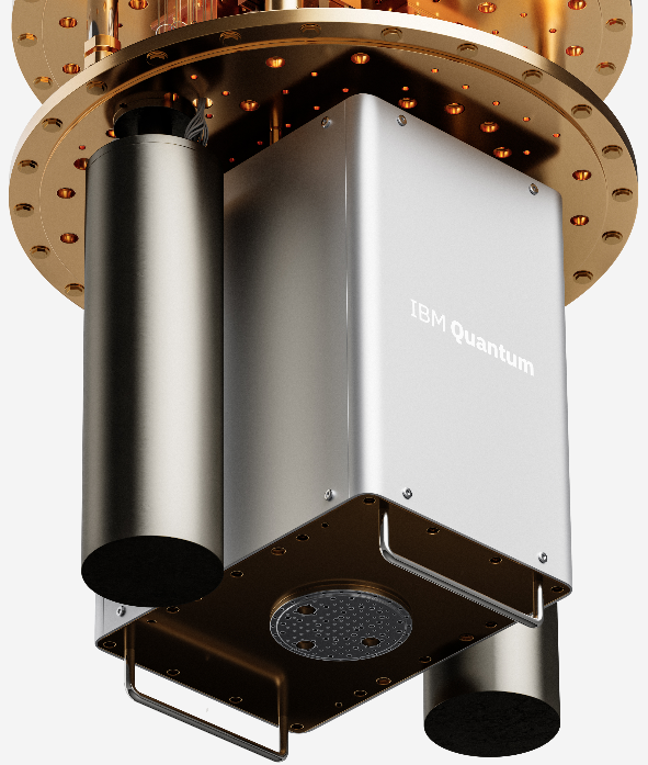
Another aspect of the applied research led by Mirhassani is hardware testing in collaboration with industry, including testing security against IBM’s quantum computer. Ansys, meanwhile, is providing simulation and pre-silicon support while CMC Microsystems is helping source faculty from its network to support the research and will also provide any hardware fabrication capabilities.

Time is short if the automotive industry is to be quantum secure, and the industry is already grappling with a great deal of uncertainty.

The funding for Mirhassani’s and other quantum research is part of a national quantum strategy launched by Canada’s federal government in 2021 to amplify the country’s strengths in quantum research, grow its quantum-ready technologies, companies and talent, as well as solidify its global leadership in quantum technologies.

Read the full EE Times article.

Gary Hilson is a freelance writer with a focus on B2B technology, including information technology, cybersecurity, and semiconductors.
Micron Drives Down DRAM Power [Byline]

March 11, 2025 / Gary Hilson

Reducing DRAM’s power footprint has always been table stakes for vendors like Micron Technology, but AI-driven data centers are putting more pressure on memory makers to make further advances in power efficiency.

Micron recently announced it is shipping samples of its 1γ (1-gamma), sixth-generation (10 nm-class) DRAM node-based DDR5 memory. The 16Gb DDR5 memory is designed to offer speed capabilities of up to 9200MT/s, a 15% speed increase compared to its predecessor, while also reducing power consumption by 20% by using next-generation high-K metal gate CMOS technology paired with design optimizations.

Micron’s sixth generation of what the company is calling its “one series” is driving performance, power, bit density and capacity improvements with each successive node. Increasing performance is always a top priority with each new node, but power reduction was a big focus for 1-gamma. These power improvements have been incremental since Micron went from 1-z to 1-alpha, with the goal of achieving double digit power reduction with every technology node.

The design of Micron’s 1-gamma has benefited from successfully integrating EUV lithography along with the company’s advanced multi-patterning techniques to achieve a 30% increase in bit density. High-K metal gate CMOS technology, meanwhile, enables better transistor performance.

Micron is the last of the “Big Three” DRAM makers to move to EUV, but was Micron was the first to use self-aligned double-patterning in the early 2000s as a means to delay the purchase of expensive immersion scanners, and did the same with EUV imagers, which cost more than $100 million each.

Micron’s 1-gamma node will first be used for its 16 Gb DDR5 DRAM and over time will be integrated across the company’s memory portfolio. Its 1-gamma samples are going out to the company’s CPU partners and select customers over the next one to two quarters as part of its technology enable program to support interoperability and qualification work across multiple platforms and segments.

Read the full EE Times article.

Gary Hilson is a freelance writer with a focus on B2B technology, including information technology, cybersecurity, and semiconductors.

Canadian Firm Unveils Quantum Error Correction Codes [Byline]

February 25, 2025 / Gary Hilson

A Canadian company has hit a significant milestone in its efforts to accelerate the timeline to useful quantum computing.

Vancouver-based Photonic Inc. has introduced a new, low-overhead family of quantum low-density parity check (QLDPC) codes, which can efficiently perform quantum computation and error correction at the same time while using materially fewer quantum bits (qubits) than traditional surface code approaches.

Unlocking the quantum logic of high-performance QLDPC codes has been the “holy grail” of quantum error correction research and development for 30 years. It is also one of the obstacles to cost-effective quantum computing at scale.

Photonic’s “fast and lean” QLDPC codes, called SHYPS codes, can run all quantum algorithms using up to 20× fewer physical qubits compared to the traditional approaches to error correction, which is a key challenge that must be addressed if quantum computing is to become widely adopted.

Error correction is necessary if quantum computing is to realize the promised exponential speedups over known classical approaches for key computational challenges.

QLDPC codes are not new; they were introduced 20 years ago, but it has taken researchers more than a decade to unlock the ability to perform quantum logic using QLDPC codes. Photonics’ new research paper outlines how to compute using SHYPS QLDPC codes and achieve efficiency gains that will lead to commercially useful quantum applications.

These error correction codes are necessary to build quantum repeaters—objects that take a quantum signal and extend the distance.

Photonic’s QLDPC code family has specific hardware requirements for implementation that not every approach to quantum computing can deliver. The company’s Entanglement First architecture provides the high levels of connectivity needed to realize the benefits of QLDPC codes.

Late last year, Photonic announced it was testing quantum networking that leverages quantum encryption for ultra-secure, tamper-evident transfer of information over long distances with one of Canada’s major telcos, Telus.

Read the full EE Times article.

Gary Hilson is a freelance writer with a focus on B2B technology, including information technology, cybersecurity, and semiconductors.

PCIe Gains Automotive Mileage [Byline]

February 12, 2025 / Gary Hilson

Microchip Technology’s latest PCIe switches are only Gen 4.0, but for automotive and industrial applications, the bandwidth is more than enough.

The company’s recently announced PCI100x family of Switchtec PCIe Gen 4.0 switches come in variants to support packet switching and multi-host applications. They also include the PCI1005, a packet switch that expands a single host PCIe port to as many as six endpoints, as well as the PCI1003, which enables multi-host connectivity through non-transparent bridging (NTB) and is fully configurable to support from four to eight ports.

The PCI100x family of Switchtec PCIe switches are Gen 5.0 compliant—Gen 7.0 was recently presented to PCI-SiG) members for review—and up to 16GT/s. But while PCIe Gen 5.0 parts are in production, Gen 6.0 adoption is in its infancy. For automotive applications, Gen 4.0 is more than enough.

In 2024, Gen 5.0 cost 50% more than Gen 4.0, but with 100% more bandwidth; a streaming scenario can take advantage of Gen 5.0, but if you do not need 32 Gb per lane, and you are not going to use it all, you are paying for what you do not need. Some defence and aerospace companies will spend more on data center grade Gen 5.0 switches in small volumes because they are using a lot of bandwidth.

The approach with automotive OEMs is not to reinvent the wheel by leveraging what has been proven in the data center for nearly 30 years while doing it through the lens of functional safety and endurance in extreme environments, both of which are critical for modern vehicle applications.

Automotive is a high priority for PCIe and the PCI-SIG is in charge of guiding its evolution, which aligns well with increasing adoption of ethernet and NVMe within the modern vehicle. PCI-SIG announced it was committed to releasing PCIe 7.0 in 2025 during the PCI–SIG Developers Conference with the aim of doubling the data rate to 128 GT/s and up to 512 GB/s bi–directionally via x16 configuration. It is now in the review phase and should be released later this year.

Read the full EE Times article.

Gary Hilson is a freelance writer with a focus on B2B technology, including information technology, cybersecurity, and semiconductors.
Onsemi’s Treo Taps Weebit ReRAM [Byline]

February 7, 2025 / Gary Hilson

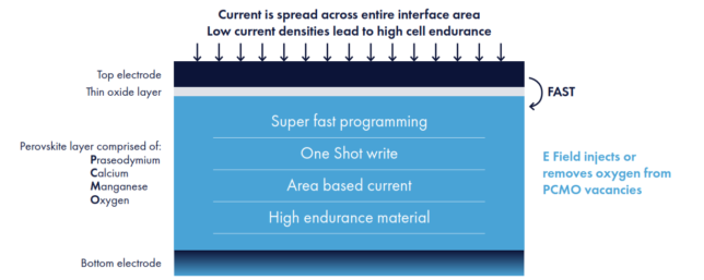
Weebit Nano’s latest licensing agreement is a significant one for the ReRAM maker, which will see its ReRAM integrated into onsemi’s Treo Analog and Mixed Signal Platform to provide it with embedded NVM.

This is the third licencing agreement for the company and a significant one revenue-wise. Onsemi’s 65-nm Bipolar-CMOS-DMOS (BCD) manufacturing facility in East Fishkill, N.Y., is shipping many different parts, but that one piece that is missing there is an NVM. TSMC was the first manufacturer to offer the ability to integrate NVM into their BCD process, and that trend has grown among vendors, foundries and IDMs. Weebit Nano already has a similar deal with DB HiTek, a global top 10 foundry.

The licensing agreement is significant for Weebit Nano because onsemi’s 65-nm platform is aimed mostly at industrial and automotive applications, the latter of which has tough certifications and environmental demands, as well as a high number of cycles before the memory fails.

ReRAM is not the only NVM that can handle the extremes of automotive, but alternatives like MRAM only make sense at more advanced process nodes. The materials, equipment and tools necessary do not make it economically feasible for anything like what onsemi is doing at 65 nm. The other alternative is embedded flash, but it is a front-end technology, making it a riskier, more expensive endeavor. As a back-end technology, ReRAM is completely separated from any analog parts on the front end, which simplifies integration and makes it low risk, making it the best option for BCD.

Power consumption is also a critical characteristic, with ReRAM coming in much lower than embedded flash—only 3 V for programming compared to 12 V for flash.

The Treo platform is the culmination of a multi-year effort, launched at electronica 2024. It integrates bipolar, CMOS and DMOS transistors on a single chip, supporting voltages from 1 V to 90 V and temperatures up to 175 degrees Celsius.

The platform has a modular, SoC-like architecture and includes numerous IP building blocks that make up the compute, power management, sensing and communications subsystems built on the 65-nm process node.

Treo also supports the industry’s widest voltage range on a leading node, and simplifies system designs, reduces costs and boosts performance for automotive, industrial and medical applications, as well as AI data centers.

Read the full EE Times article.

Gary Hilson is a freelance writer with a focus on B2B technology, including information technology, cybersecurity, and semiconductors.

Quantum Headlines Western Canada’s Semiconductor Scene [Byline]

January 6, 2025 / Gary Hilson

Western Canada’s semiconductor diversity can be boiled down to density—the most western province of British Columbia benefits from its geographic alignment with Silicon Valley. Meanwhile in the east, Manitoba is a single university province that is primarily a user of chip technology.

What all provinces have in common is strong academic institutions with relevant training and research capabilities that can contribute to Canada’s semiconductor industry, including its burgeoning quantum computing capabilities.

Located right next to Canada’s most densely populated province of Ontario, Manitoba is home to the research-intensive University of Manitoba.

The province of Saskatchewan next door is also relatively small, but home to Canada’s only synchrotron—the Canadian Light Source based at the University of Saskatchewan, which is used by scientists within the fields of health, agriculture, energy, the environment, and advanced materials.

The other end of western Canada is arguable the densest in terms of academic research and commercial semiconductor activity, which is heavily focused on quantum computing. Simon Fraser University (SFU), located in the Vancouver-adjacent city of Burnaby, is home to 4DS Labs—SFU’s core facility for advanced materials research and development, which provides access to its tools to industry through a fee-for-service model.

The lab recently received a CDN $4.5 million (about $3.1 million) grant from the Canadian federal government to invest in quantum computing manufacturing equipment, which will help a lot of small companies.

4DS Labs is one of several facilities that support researchers and industry in western Canada. The University of British Columbia is home to the Quantum Materials Institute, while one province to the east houses the Alberta Create Center, affiliated with the University of Alberta in Edmonton and its nanoFABFabrication & Characterization Centre. The university also supports quantum technologies and is home to the National Research Council’s Nanotechnology Research Centre.

Alberta’s other major center, Calgary, is home to the Institute for Quantum Science and Technology at the University of Calgary and hosts 21 research groups and about 140 academic members, including professors, research staff and students. The university is also home to Quantum City, which is building an ecosystem for quantum science and technology together with researchers and developers, as well as industry and adopters of quantum technology and services.

Read the full EE Times story

Gary Hilson is a freelance writer with a focus on B2B technology, including information technology, cybersecurity, and semiconductors.
CXL Update Emphasizes Security [Byline]

January 3, 2025 / Gary Hilson

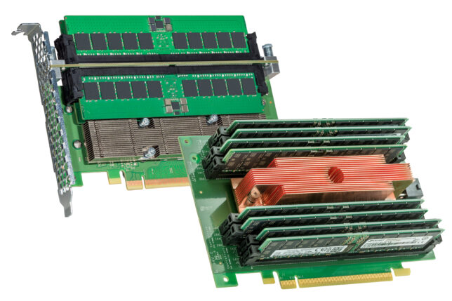
The latest point release to the Compute Express Link specification aims to optimize monitoring and management and enhance functionality for operating systems and applications—all while extending security.

The updates reflect the rapid growth of AI in the data center, even though the coherent connectivity protocol was conceived before the AI boom took off.

The latest CXL update, CXL 3.2, adds several monitoring and management capabilities, including a CXL hot-page monitoring unit (CHMU) for memory tiering, common event record, compatibility with PCIe management message pass through (MMPT) and CXL online firmware (FW) activation.

CHMU enables software to identify hot pages in second-tier memory and migrate them to first tier, such as DDR DRAM, to improve power and performance of the tiered memory solution. New common event record capabilities allow for improved granularity, monitoring precision and management of complex CXL device configurations, which enhances overall system performance and resource allocation.

Additional functionality in 3.2 includes post package repair (PPR) enhancements and performance monitoring events for CXL memory devices.

The trusted security protocol (TSP) features first introduced in CXL 3.1 are in line with confidential computing concepts pioneered by Intel that predate CXL and allow for virtualization-based trusted execution environments to host confidential computing workloads. Additional TSP features in 3.2 include IDE protection for late poison messages, which improves security for CXL-attached systems by allowing late poison messaging authentication using IDE.

The CXL interconnect has evolved rapidly since its debut in 2019 with three sub-protocols: CXL.io, CXL.cache and CXL.memory. CXL.io is necessary for I/O instructions. The first iteration supported direct attachment of memory, while 2.0 added the capability to attach memory to a pool of processors, allowing for the use of storage-class memory or persistent memory, or tiers of memory with different performances and cost structures.

CXL 3.0 supports more disaggregation with advanced switching and fabric capabilities, efficient peer-to-peer communications, and fine-grained resource sharing across multiple compute domains.

Read the full EE Times story

Gary Hilson is a freelance writer with a focus on B2B technology, including information technology, cybersecurity, and semiconductors.
Micron, Intel Bring MRDIMM Modules to Market

August 16, 2024 / Gary Hilson

Micron Technology’s latest memory offering is a collaboration with Intel to address memory-intensive data center applications like AI and high-performance computing (HPC).

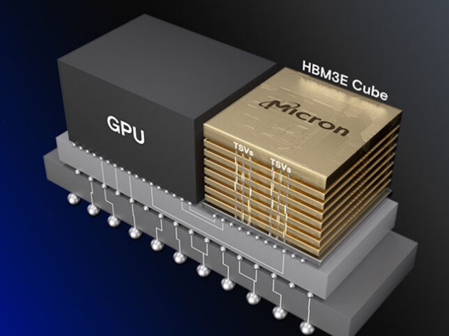
Micron presented its multiplexed rank dual inline memory modules (MRDIMMs). This first generation of MRDIMMs will enable customers to run increasingly demanding workloads with support for a wide capacity range from 32 GB to 256 GB in standard and tall form factors (TFF), which are suitable for high-performance 1U and 2U servers, and are compatible with Intel Xeon 6 processors.

For applications requiring more than 128 GB of memory per DIMM slot, Vaidyanathan said Micron MRDIMMs outperform current TSV RDIMMs, while the TFF modules feature an improved thermal design that reduces DRAM temperatures by up to 20 degrees Celsius at the same power and airflow to enable more efficient cooling in the data center.

Over the last decade, compute performance has been delivered through rapid growth in core count to grow system bandwidth, but the challenge has been maintaining bandwidth per core and getting it to curve upward. The MRDIMM is Micron’s effort to reduce the decline in bandwidth per core, he added.

Compared with RDIMMs, MRDIMMs increase in effective memory bandwidth as much as 39% and latency by 40%, while offering 15% better bus efficiency.

Micron and Intel confirmed that its MRDIMM product would be in alignment with industry standards—it implements DDR5 physical and electrical standards that scales both bandwidth and capacity per core to future-proof compute systems.

The Intel/Micron launch came out ahead of the JEDEC Solid State Technology Association revealing key details about its upcoming standards for DDR5 MRDIMMs, which it said would enable applications to exceed DDR5 RDIMM data rates. Other planned features in the JEDEC MRDIMM standard will include platform compatibility with RDIMM for flexible end-user bandwidth configuration, use of standard DDR5 DIMM components like DRAM, DIMM form factor and pinout, serial presence detect (SPD), power management integrated circuits (PMIC), and temperatures sensors (TS) for ease of adoption.

JEDEC said there are also plans to support the tall MRDIMM form factor to offer higher bandwidth and capacity without changes to the DRAM package. By going taller, it is possible to enable twice the number of DRAM single-die packages to be mounted on the DIMM without the need for 3DS packaging.

Read my full story on EE Times.

Gary Hilson is a freelance writer with a focus on B2B technology, including information technology, cybersecurity, and semiconductors.

DPUs take the pressure off purpose-focused processes [Byline]

August 14, 2024 / Gary Hilson

Data processing units (DPUs) are having a moment.

As artificial intelligence (AI), high performance computing (HPC), increasingly complex cloud architectures and security demands put more pressure on central processing units (CPUs), and graphics processing units (GPUs), DPUs have stepped up their game.

In baseball parlance, DPUs can be seen as a “utility player,” in that they can be deployed in different ways to support workload-focused players – the CPUs and GPUs. DPUs can trace their history to the Smart network interface card (SmartNIC), which were initially designed to offload some network functions from the CPU to improve network traffic flow.

But traditional SmartNICs aren’t smart enough proceed the high volumes and different patterns of data that DPUs can. The democratization of AI through ChatGPT has put a lot of pressure on the backend as frontend users began consuming it faster – once it hit a tipping point, everyone was using it. Not all DPUs are created equal however, and AI is just one use case that’s driving their adoption.

One position DPUs can play is security. In September 2022, Nvidia introduced a DPU designed to implement zero-trust security distributed computing environments, both in the data center and at the edge. Nvidia’s BlueField-2 DPUs were specifically tailored to be used Dell PowerEdge systems with the aim of improving the performance of virtualized workloads based on VMware vSphere 8.

Nvidia’s Bluefield-3, meanwhile, is the equivalent of 300 CPU cores, and it employs purpose-built accelerators to handle storage, security, networking and steering traffic.

The next generation of AI is AI agents talking to other AI agents, and DPUs play a key role in automation and scalability while humans continue to increasingly interact with AI.  Nvidia is building out a microservices platform, NIM, that leverage DPUs to orchestrate AI interactions, providing containers to self-host GPU-accelerated inferencing microservices for pretrained and customized AI models.

The utility of DPUs in modern AI data centers has meant that other players beyond semiconductor vendors are seeing the value of owning their own DPU technology. Microsoft acquired Fungible to integrate its DPU technology into its data center infrastructure – it was already using DPUs in Azure, and there are plenty of options. Aside from Nvidia, Intel, Broadcom and AMD all have DPU offerings. Amazon Web Services, meanwhile, has its own DPUs, dubbed “Nitro.”

AMD bulked up its DPU capabilities in 2022 with the acquisition of Pensando and its distributed services platform, which had a footing in Azure, IBM Cloud and Oracle Cloud. The Pensando acquisition means AMD finds its DPU adopted in several hyperscale cloud providers. It has also been incorporated into smart switches from Aruba and Cisco.

Taking on front-end networking functions to securely connect to the GPU continues to be a key role for DPUs, as well as enabling secure isolation in multi-tenant hyperscale cloud data centers. The DPU can also accelerate storage access and speed up data ingestion – the increased volumes of training data are driving speed and performance requirements, and hence more offloading to the DPU.

With the explosive growth of generative AI, networking is the currently bottleneck as the number of GPUs in data centers grow, which is why DPUs are essentially for managing data traffic and taking on functions so the GPUs can focus on application workloads.

Read my full story on Fierce Electronics.

Gary Hilson is a freelance writer with a focus on B2B technology, including information technology, cybersecurity, and semiconductors.

Posts pagination

1 2 … 18 Next »

Recent Posts

  • SoCs Get a Helping Hand from AI Platform FlexGen [Byline]
  • Canada Funds Quantum Auto Security Research [Byline]
  • Micron Drives Down DRAM Power [Byline]
  • Canadian Firm Unveils Quantum Error Correction Codes [Byline]
  • PCIe Gains Automotive Mileage [Byline]
  • Onsemi’s Treo Taps Weebit ReRAM [Byline]
  • Quantum Headlines Western Canada’s Semiconductor Scene [Byline]
  • CXL Update Emphasizes Security [Byline]
  • The Painful Art of Accepting Life’s Stalemates
  • Micron, Intel Bring MRDIMM Modules to Market

Recent Posts

  • SoCs Get a Helping Hand from AI Platform FlexGen [Byline]
  • Canada Funds Quantum Auto Security Research [Byline]
  • Micron Drives Down DRAM Power [Byline]
Powered by WordPress | Theme by Themehaus